Nomenclatures and Abbreviations that you Should Know in PCB
Printed Circuit Boards are the veins of an electronic device. They act as a carrier on which sits multiple components and connections essential for making the electronic device run. However, due to multiplicity of components and processes, we tend to forget or unaware of some their name and utility.
In this article all the relevant nomenclatures, whether part or abbreviation or a process or a connection, are all enlisted and defined.
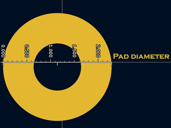
Annular Ring
This term refers to the copper pad area that is left after a hole is drilled through it. This ring is measured from the edge of the pad to the edge of the hole and is an important consideration in PCB design, as it allows an electrical connection to be made from one side of the hole to the other.
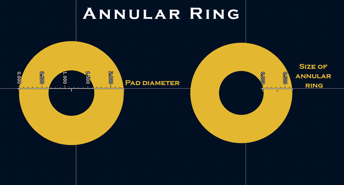
Annular ring
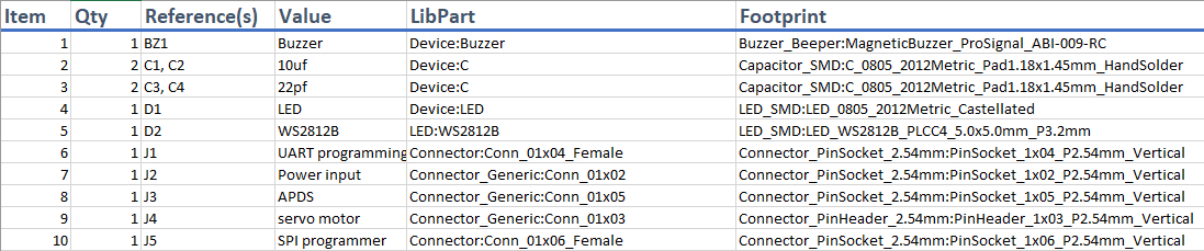
Bill of Materials (BOM)
A bill of materials or BOM is a standard means of listing all of the items required to build or construct a structure. For the PCB construction process, the BOM is actually an electronics component list that provides information essential for the accurate placing of components on your board.
Bill of Material
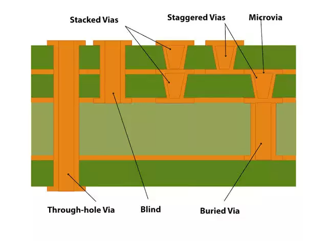
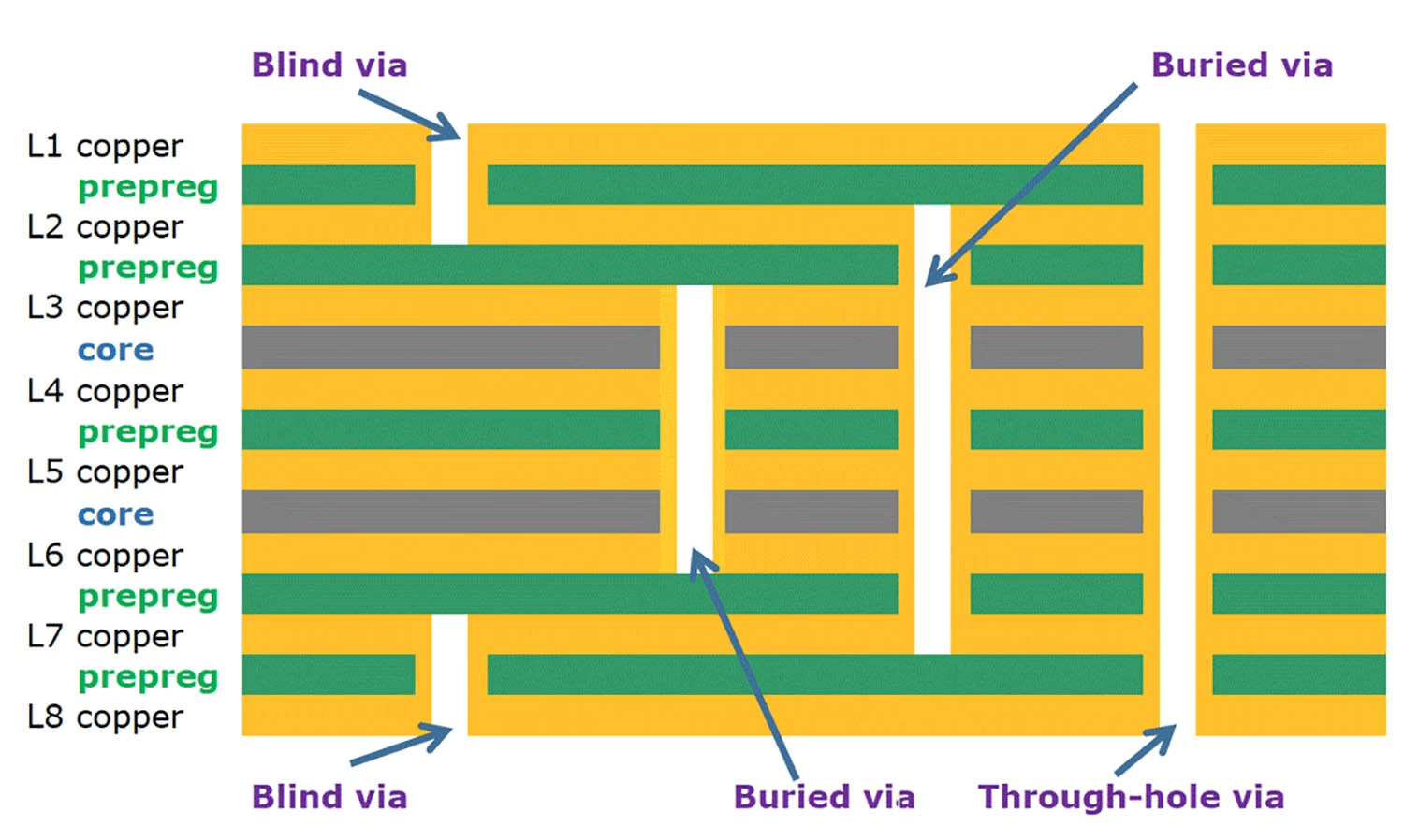
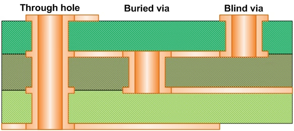
Blind Via
A blind via is a through-hole that connects inner layers, but it can’t be seen from the exterior of the PCB.
Blind Via
Buried Via
It refers to a via connecting a top layer to one or more inner layers. In other words, a buried via can only be seen from one side of the board when looking at it from the outside.
Buried Via
Board Thickness
It is the total height of the board; not including components. It is well-known that the size (in the horizontal plane) of circuit boards has been decreasing to accommodate the demand for smaller electronic devices and products.
Board thickness
Castellated Holes
Holes that are drilled on the edge of a board and plated, resulting in a half-circle hole on the edge of the PCB. It allows the board to be soldered onto another board.
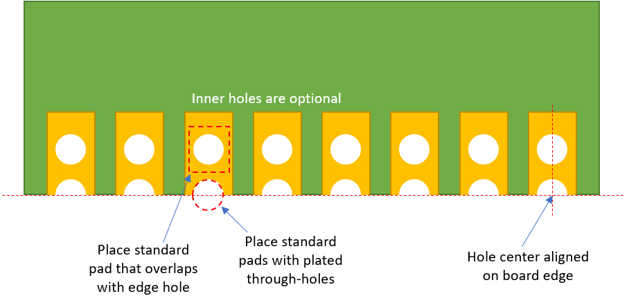
Castellated Holes
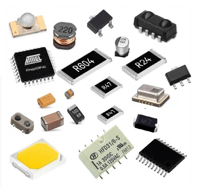
Components
Electronic components are basic pieces that can be used to build electronic equipment and devices. Examples include resistors, capacitors, potentiometers, valves, transistors, etc.
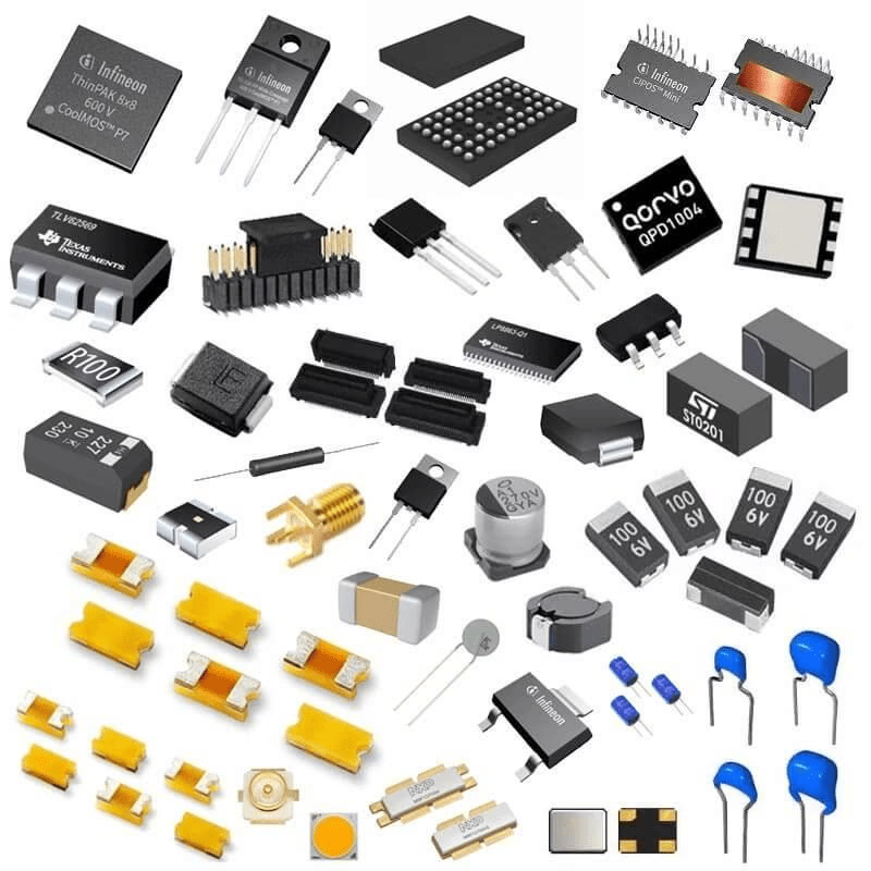
Electronic components
Connector
This term refers to a transmitting component that connects two or more active components in an assembly. They consist of a plug and receptacle, which can be easily joined and separated.
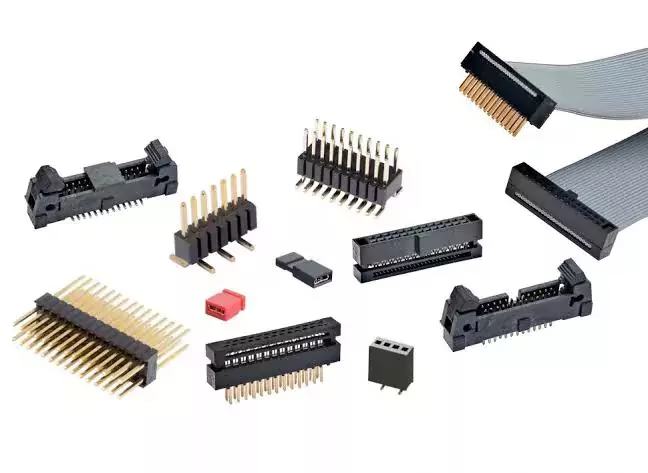
Connectors
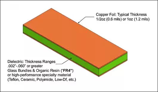
Copper Weight
This term is used to indicate thickness of copper foil on each layer of a PCB. It’s typically expressed in ounces of copper per square foot.
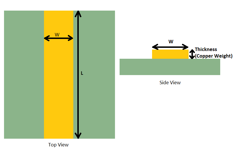
Copper weight
Countersink Holes
Cone-shaped holes that are drilled into a PCB. To allow a countersunk screw to sit flush with the PCB surface.
Countersink holes
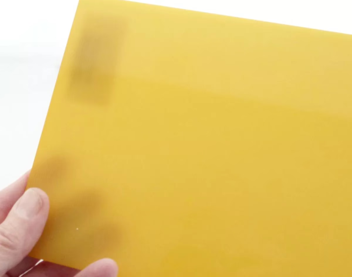
Clad
Clad references the material used in manufacturing PCBs. Fiberglass material is “clad” with copper and is used as the starting place for manufacturing of the PCB.
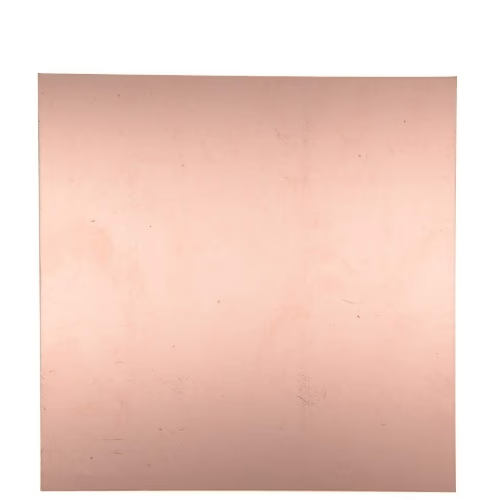
Clad
Clearance
It is defined as the shortest distance between two points on a PCB or the trace (for example, a component to the edge of the board, through the air).
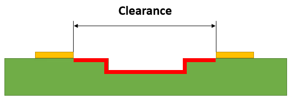
Clearance
DIP
An abbreviation for a Dual-In-Line Package, a DIP is a kind of housing for integrated circuits. This housing will typically come in the form of a molded plastic container with two rows of attachment pins.
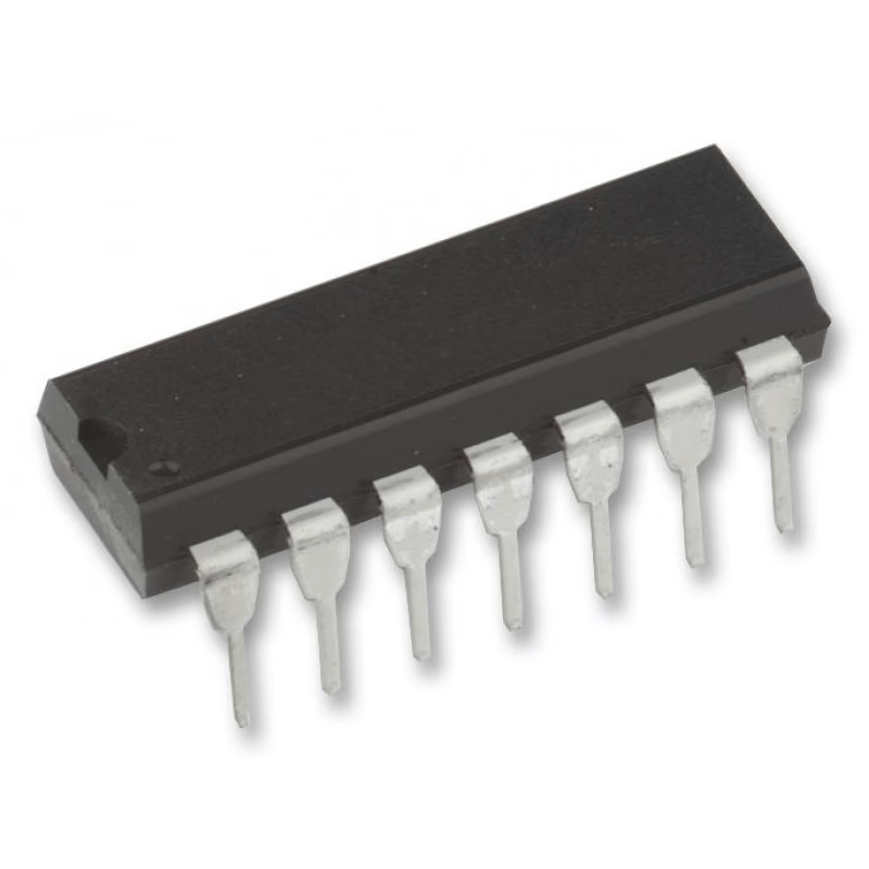
DIP
DRC
Design Rule Check, is a software verification of a PCB layout. It is used on PCB designs before production to ensure the design doesn’t contain any potential sources of error, like small drill holes or traces placed too close together.
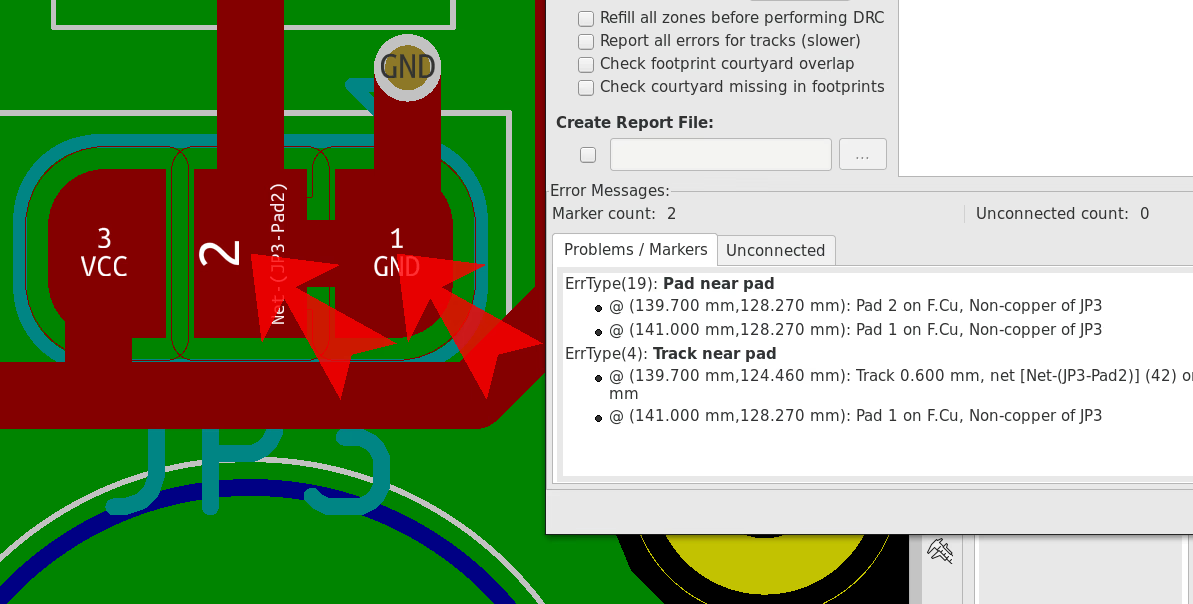
PCB Design Rule Check
ESD
A shorthand for Electrostatic Discharge, which is caused by static electricity.
ESD on PCB
Etching
After an circuit design has been applied to a panel of copper clad fiberglass the unwanted copper is chemically etched away to make the traces.
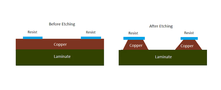
Etching
Footprint
It is a pattern for an electronic component that will eventually be soldered there. Often referred to as landing patterns, these footprints and their arrays of metal pads are to what the electronic components will be soldered.
Footprint
FR4
This is a material rating for a flame-resistant material. It also refers to the most commonly used PCB substrate material. The name specifies that the resin material is capable of automatically extinguishing when it is aflame.
FR4 Material
Gerber File
A design file that is used in production / fabrication of PCB. It is a CAM file used to control a photoplotter. It’s a standard way of communicating board specifications with manufacturers.
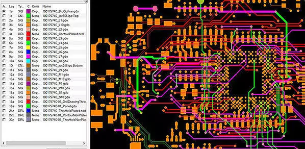
Gerber file
Gold Fingers
Connectors found on the edge of a PCB after the board has been plated with gold. Hard, smooth and flat, these fingers are excellent conductors, supporting edge-to-edge connections.
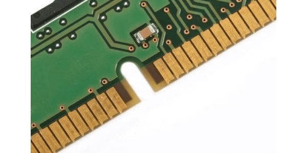
Gold Fingers
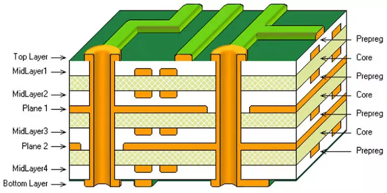
Layers
Everything on which a PCB is designed is on a layer. Each layer has different physical properties. For example top layer is used to draw the component layout, bottom layer or inner layer are used for making connections between components and many more are also present.
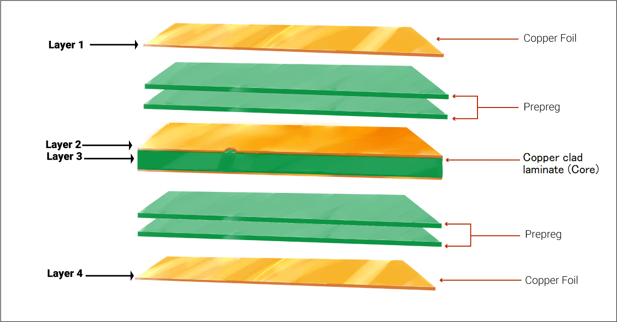
PCB Layers
Mounting Hole
This hole is intended to secure the PCB to its final location in a device. To ensure there is no interference, all mounting holes are non-conductive and unplated.
Mounting holes on PCB
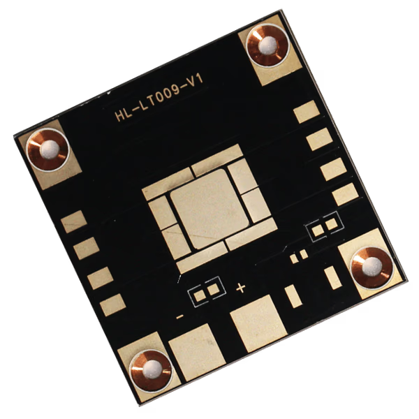
Multi-Layer PCB
It is a PCB with multiple conductive layers of trace and components. Multiple layers stacked one after the other.
Multilayer PCB
Netlist
List of names of symbols or parts and their connection points which are logically connected in each net of a circuit.
PCB Netlist
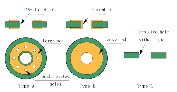
Non-Plated Through Holes (NPTHs)
Non-copper plated PCB drill holes used to mount or install boards in enclosures or other devices.
Non-plated through holes
Pad
This is one of the most basic composition units of a PCB assembly. A pad is a contact used to connect components. It is the point to which the components are soldered.
Pads
Panel
A panel is a combination of boards produced simultaneously to improve scalability during the manufacturing process. Once the process is finished, these panels are typically broken apart into their singular units before being used.
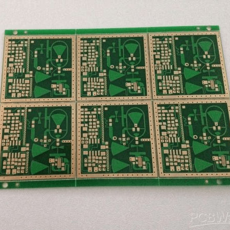
Panel
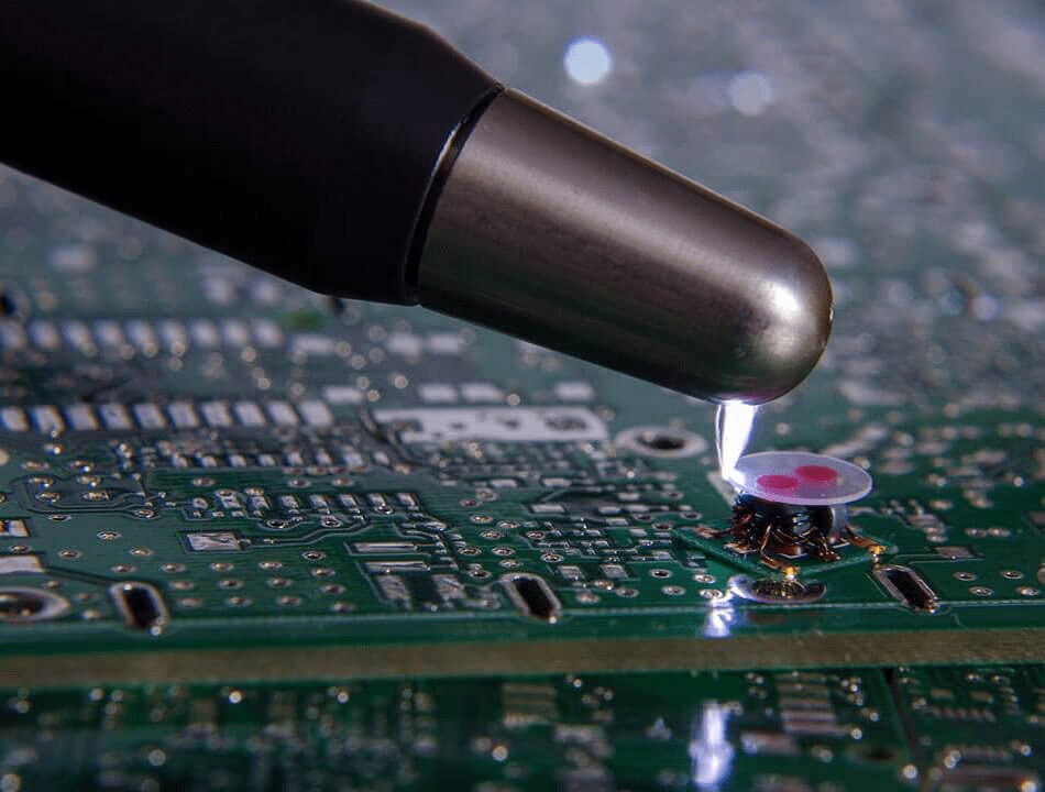
PCBA
Printed Circuit Board Assembly is the process where the manufactured boards are assembled to make a working circuit. It includes placement and soldering of components to boards.
PCB Assembly
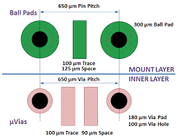
Pitch
The distance between successive pins or pads of a component or footprint is called pitch.
Pitch
Plated Through Hole (PTH)
It is used to carry current vertically through the board. These vias are also used to aid in heat dissipation.
PTH
RoHS
Restriction of Hazardous Substances, RoHS is a European environmental protection law. Many global companies must follow RoHS standards to sell products in the EU.

Restriction of Hazardous Substances
Silkscreen
This is a layer of epoxy ink applied to a PCB that contains component names and positions. The labels included on silkscreens help to direct workers through the assembly process. Typically, silkscreens are white, which helps the labels stand out against the PCB’s solder mask.

Silkscreen
Surface Mount Devices
These are components in which the pins or leads are soldered to the surface of a circuit board. This includes flat packages, BGAs and CSPs, where connections to the component are underneath.
Surface mount devices
Surface Finish
Copper tends to oxidize in natural environments, a surface finish protects the layer from doing so. Oxidation can cause the tin paste to fail or solder incorrectly. The primary types of surface finishes include HASL, ENIG, IMAG, OSP and others.
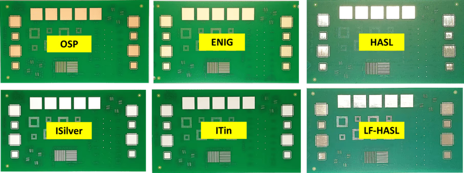
Surface finish for PCB
Via
This term refers to plated through-holes that connect signals between traces on different layers of a PCB. These holes have conductive copper interiors to maintain an electrical connection.
Via
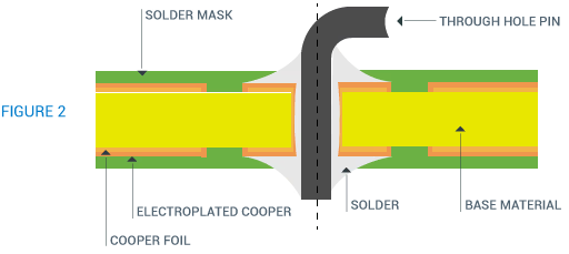
V-Scoring
This is an incomplete cut through a panel, which is often used to help break apart panels of PCBs into single units.
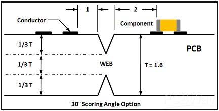
V-Scoring
These are the most frequently used terms in electronic lexicon which an PCB Design engineer should be aware of. These terms are useful from the designing process to the assembly of PCB. Having a clarity about the basics always helps in communicating better and enhances our learning experience.